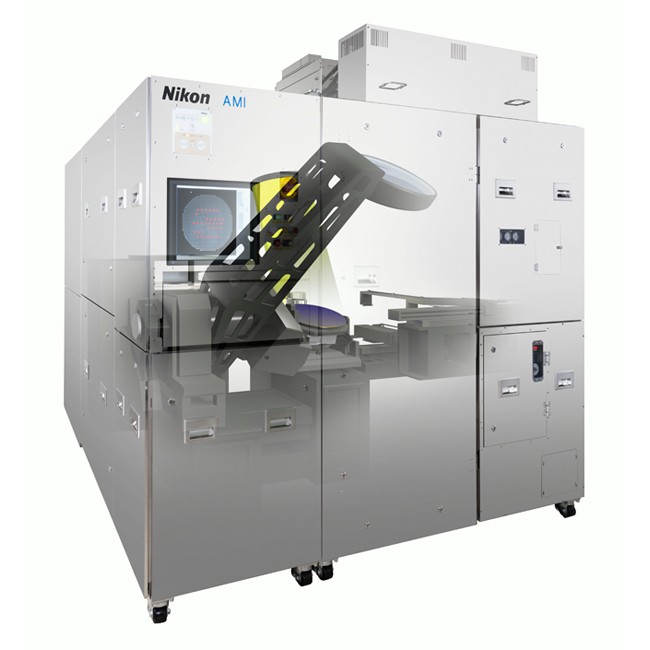
AMI-5700

▉▉ Nikon's diffracted light detection system detects pattern variations along the Z-axis, especially focus error and poor coating, with high sensitivity. In addition, accurate recognition of the diffracted light only from the top pattern layer is possible, allowing defects in underlying patterns to be discriminated.
▉▉ High quality images with reduced chromatic aberration can be obtained by the newly developed optical system and improved collection mirror.
▉▉ An improved mirror tilting mechanism greatly contributes to the reduction of under - layer noise, realizing more accurate inspection, such as the accurate detection of changes in the top layer pattern.
▉▉ Detects particles and scratches as small as 5 um by scattering inspection, achieving even higher sensitivity than previous models.
▉▉ Achieves high throughput of 180 wafers/hour, even when performing diffraction and scattering inspection as a batch inspection of the entire wafer. Also supports 3 load ports and enables efficient operation according to the line,greatly contributing to improved productivity.
▉▉ A high-speed measurement function has been implemented for the first time in the AMI series. CD measurement, film thickness measurement and focus measurement are possible at speeds that surpass previous methods.
▉▉ Complies with the RoHS directive and REACH regulations concerning the environment.
▉▉ A unique leaming function utilizes AI image processing technology to quantify the characteristics of a good wafer.
▉▉ The versatile automatic recipe creation function allows even inexperienced operators to create optimal recipes in a short time.
▉▉ In addition to the Automatic Defect Classification(ADC)function,operators can specify their own rework criteria in a recipe in order to automate rework judgments.
▉▉ Hole process inspections are also supported.

